TXMC638

Reconfigurable FPGA with Analog Input

  • Standard XMC module
  • User configurable FPGA (AMD Kintex™ 7)
  • 1 Gbyte, 32 bit wide DDR3 SDRAM
  • 24 channels 16 bit ADC
    • Offering single-ended and differential mode
    • single-ended voltage input ranges (±2.5 V)
    • differential voltage input ranges (±5 V)
    • Sampling rate up to 5 Msps
  • Digital rear I/O
    • 64 single ended digital I/O lines (LVCMOS25)
      or 32 differential digital I/O lines (LVDS25)
  • Front panel I/O (Rugged EdgeRate connector) and rear I/O via P14 and P16

Product status: Active

Operating Temperature Range -40 °C to +85 °C RoHS compliant

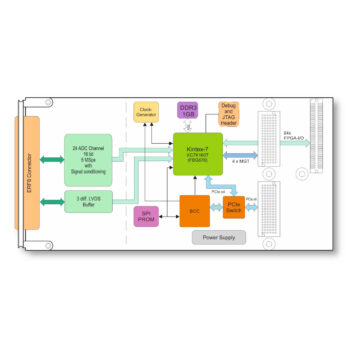
The TXMC638 is a standard single-width Switched Mezzanine Card (XMC) compatible module providing a user configurable AMD Kintex™ 7 FPGA with 24 ADC input channel.

The TXMC638 ADC input channels are based on the Linear Dual 16-Bit 5Msps Differential LTC2323-16 ADC. Each of the 24 channels has a resolution of 16bit and can work with up to 5 Msps. The analog input circuit is designed to allow input voltages up to ±2.5 V on each input-pin (results in ±5 V differential voltage range)

For customer specific I/O extension or inter-board communication, the TXMC638 provides 64 I/Os on P14 and 4 Multi-Gigabit-Transceiver on P16. The P14 I/O lines are connected directly to the FPGA and can be used as 64 single ended LVCMOS25 or as 32 differential LVDS25 interface be using I/O configuration of the FPGA.

Additionally the TXMC638 provides three 100 Ohm terminated ac-coupled, differential inputs with wide Input voltage range.

All these front I/O lines like the ADC interface and the three 100 Ohm inputs are connected to a 98-pin. Samtec ERF8-049 Rugged EdgeRate Connector.

A 1 GB, 32 bit wide DDR3 SDRAM is connected to the User FPGA. The SDRAM-Interface uses an internal Memory Controller of the Kintex 7.

The User FPGA is configured by a serial SPI flash. For full PCIe specification compliance, the XILINX Tandem Configuration Feature can be used for FPGA configuration. XILINX Tandem Methodologies Tandem PROM should be the favored Methodology. The SPI flash device is in-system programmable.  An in-circuit debugging option is available via a JTAG header for read back and real-time debugging of the FPGA design (using Xilinx ChipScope).

User applications for the TXMC638 with AMD Kintex™ 7 FPGA can be can be developed using the AMD Vivado™ design tool. A license for the Vivado Design Suite design tool is required.

TEWS offers a well-documented FPGA Board Reference Design. It includes a constraint file with all necessary pin assignments and basic timing constraints. The FPGA Board Reference Design covers the main functionalities of the TXMC638.

The TXMC638 is delivered with the FPGA Board Reference Design. The user FPGA could be programmed via the on-board Board Configuration Controller (BCC). Programming via JTAG interface using an XILINX USB programmer is also possible. In accordance with the PCI specification and the buffering of PCI header data, the contents of the user FPGA can be changed during operation.
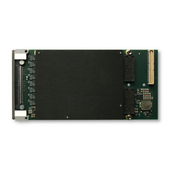
Mechanical Interface Switched Mezzanine Card (XMC) Interface confirming to ANSI/VITA 42.0-2008 (Auxiliary Standard); Standard single-width (149mm x 74mm)
Electrical Interface PCI Express x4 Link (Base Specification 2.1) compliant interface conforming to ANSI/VITA 42.3-2006 (XMC PCI Express Protocol Layer Standard)
PCI Express Switch PI7C9X2G312GP (Pericom)
PCI Express to PCI Bridge XIO2001 (Texas Instruments)
User configurable FPGA TXMC638-10R: XC7K160T-2FBG676I (AMD Kintex™ 7)
TXMC638-11R: XC7K325T-2FBG676I (AMD Kintex™ 7)
TXMC638-12R: XC7K410T-2FBG676I (AMD Kintex™ 7)
SPI-Flash N25Q128A (Micron) 128 Mbit (contains TXMC638 FPGA Board Reference Design) or compatible; +3.3 V supply voltage
DDR3 RAM 2 x MT41K256M16HA-125 (Micron) 256 Meg x 32 Bit
Board Configuration Controller LCMXO2-7000HC (Lattice)
ADC LTC2323IUFD-16 (Linear Technologies)
Number of analog Input 24 differential 16 bit Inputs
Analog Input Voltage diff. VINMAX (allowed voltage between input pins): ±5.0 V
Common Mode Voltage Range :±7.5 V
Input Voltage limit for each pin relative to common ground ±10 V
Number of digital Front I/O Three differential Front I/O Inputs with wide Input voltage range.
Differential voltage range: ±200 mV up to ±3.6 V
Differential Termination = 100 Ohm
Number of digital Back I/O 64 direct FPGA I/O lines to P14 Back I/O connector
– Possible use as single ended or differential I/O
– FPGA I/O Standard: LVCMOS25, LVTTL25 and LVDS_25
I/O Connectors Front I/O Samtec ERF8-049-01-L-D-RA-L
PMC P14 I/O (64 pin Mezzanine Connector)
XMC P16 I/O (114 pin Mezzanine Connector)
Power Requirements Depends on FPGA design
With TXMC638 Board Reference Design / without external load
3.0 A typical @ +5 V VPWR
1.25 A typical @ +12 V VPWR
Temperature Range Operating: -40 °C to +85 °C
Storage: -40 °C to +85 °C
MTBF 269 000 h
Humidity 5 – 95% non-condensing
Weight 133 g


PRODUCT VARIATIONS

TXMC638-10R

Reconfigurable FPGA with 24 Analog Input

AMD Kintex ™ 7 FPGA (XC7K160T-2 FBG676); 1 GB DDR3; 24 Analog Inputs; 64 direct FPGA Back I/O Lines on P14; 4 MGTs on P16

TXMC638-11R

Reconfigurable FPGA with 24 Analog Input

AMD Kintex ™ 7 FPGA (XC7K325T-2 FBG676); 1 GB DDR3; 24 Analog Input; 64 direct FPGA Back I/O Lines on P14; 4 MGTs on P16

TXMC638-12R

Reconfigurable FPGA with 24 Analog Input

AMD Kintex ™ 7 FPGA (XC7K410T-2 FBG676); 1 GB DDR3; 24 Analog Input; 64 direct FPGA Back I/O Lines on P14; 4 MGTs on P16

ACCESSORIES

32 Pair Twinax Cable

RJ45 Terminal Block

Cable Kit for Modules with Samtec Edge Rate Connector

SOFTWARE

Device Driver for Board Family with Reconfigurable FPGA

Data Sheet

Data Sheet

Data Sheet - Issue 1.0.4

User Manual

User Manual - Issue 1.0.1