

TPCE646

Reconfigurable MPSoC with 32 x 16 bit Analog Output and 8 x 16 bit differential Analog Input

  • Form Factor: X8 PCIe
    • Board size: 98 mm x 154 mm
  • PCI Express x8 Gen 3 Link from PCIe Card edge connector to MPSoC PL.
  • Optional PCI Express x4 Gen2 Link to MPSoC PS.
  • AMD Zynq™ UltraScale+™ XCZU11EG-1FFVC1760I
  • Serial Flash for MPSoC Configuration
  • FPGA clock options:
    • Local clock generator as source for the MPSoC internal PLL
  • DDR4 SDRAM PL bank, 64 bit 4 GB
    • (up to 8 GB)
  • DDR4 SDRAM PS bank, 64 bit 4 GB
    • (up to 8 GB)
  • 8 MPSoC PS Multi-Gigabit-Transceiver on a seperate Samtec FireFly© connector.
  • Front I/O lines
    • 8 differential analog inputs
      • 16 bit resolution
      • 5 Msps
    • 32 differential analog outputs
      • 16 bit resolution
      • ±10 V single ended output
    • 4 differential digital LVDS I/O lines
  • Rear I/O lines
    • 64 single ended or 32 differential rear I/O lines on a rear 68 pin Samtec QTE© connector.
    • 8 MPSoC PS Multi-Gigabit-Transceiver on two seperate rear Samtec FireFly© connector.
    • 10/100/1000 Mbps RJ45 Ethernet Interface

Product status: Active

RoHS complaint

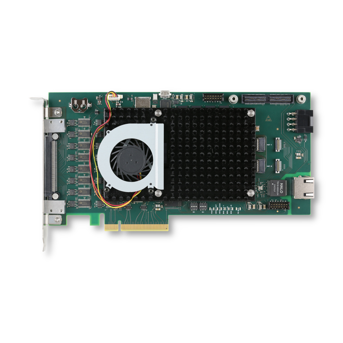
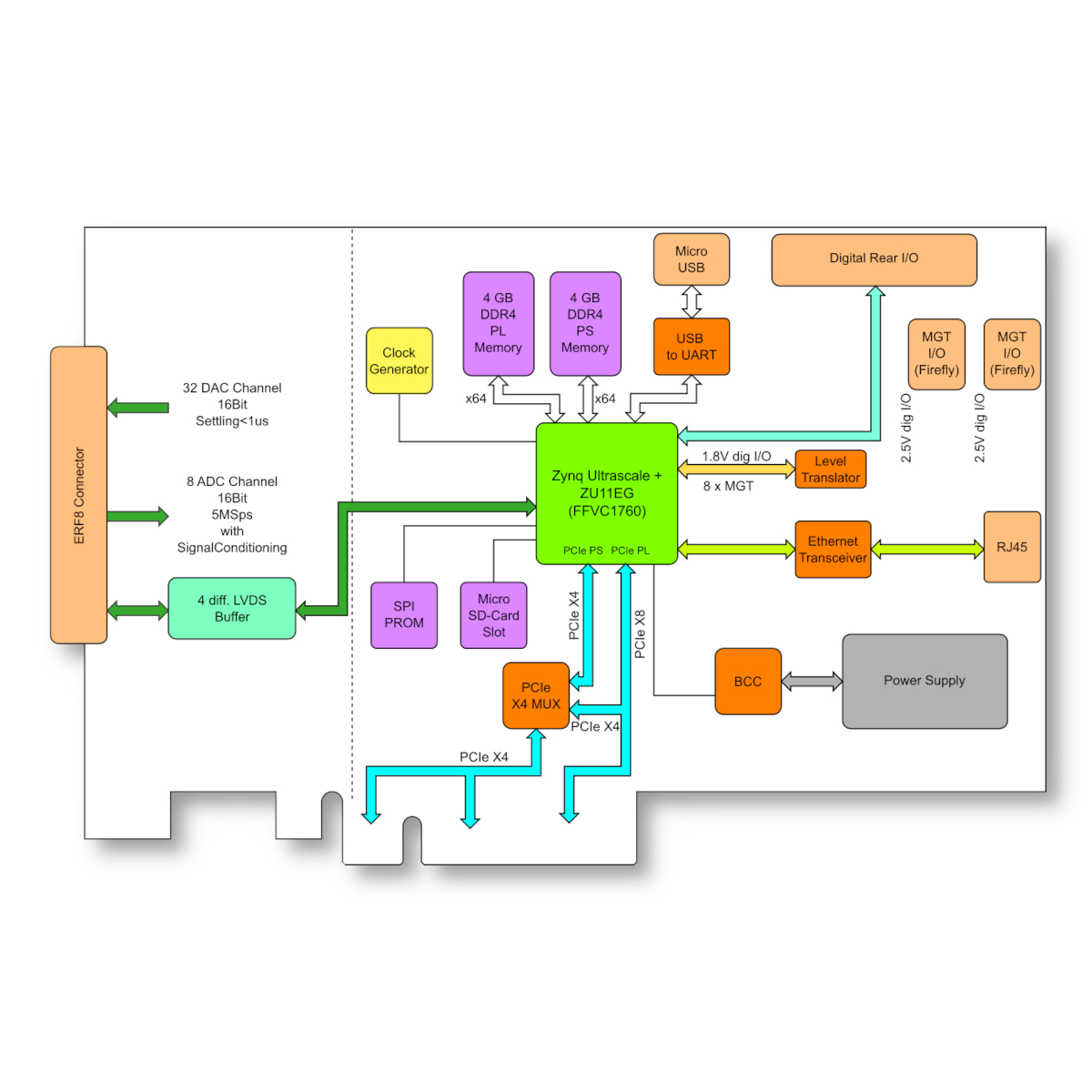
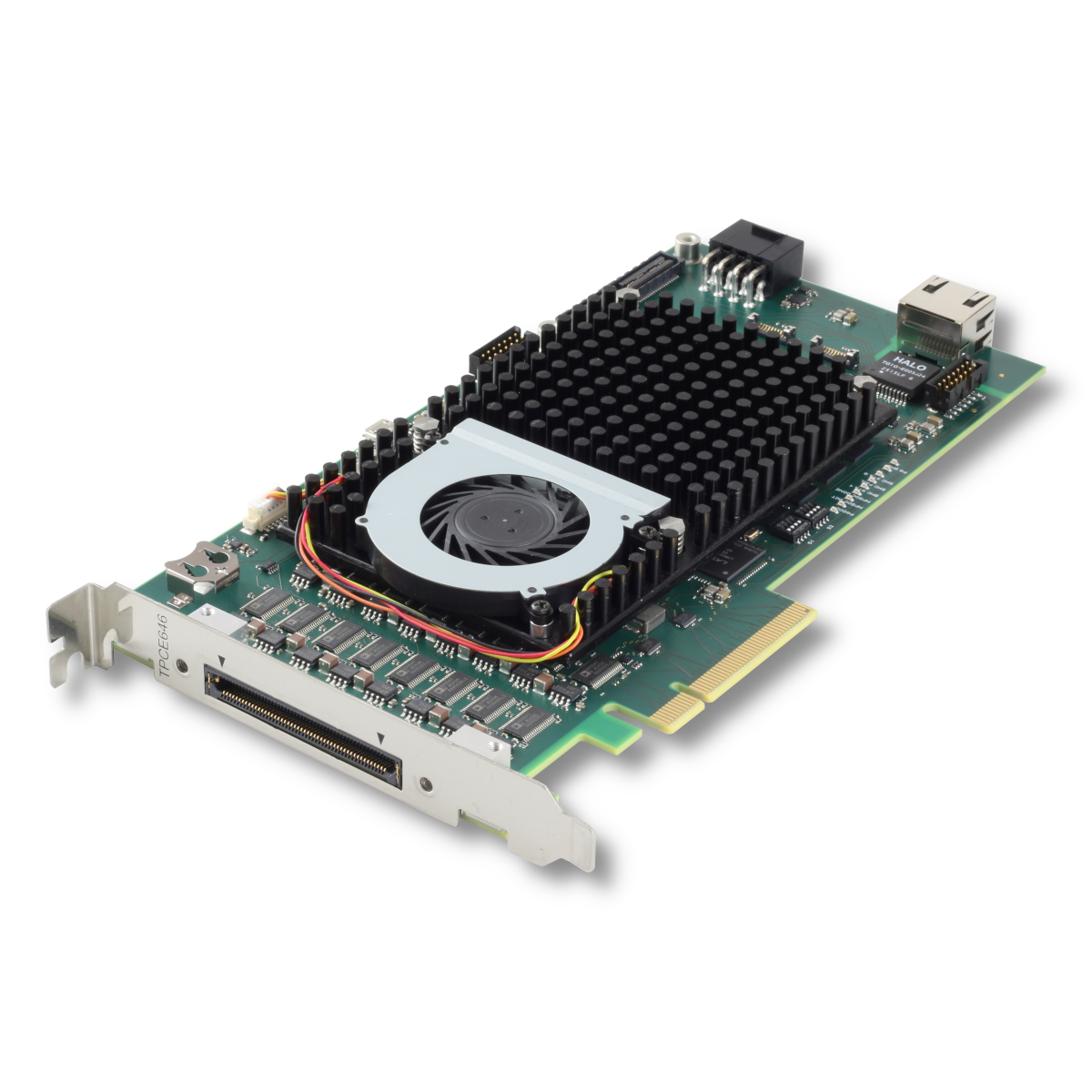
The TPCE646 is an X8 PCIe–compatible module featuring a user-configurable AMD Zynq™ UltraScale+™ MPSoC. It provides 32 DAC output channels based on dual 16 bit AD5547 DACs, each designed as a single-ended bipolar ±10 V analog output. The module also includes 8 ADC input channels using dual 16 bit LTC2323-16 ADCs, supporting up to 5 Msps per channel with a ±10 V input range (±20 Vpp differential).

Additionally, the TPCE646 offers four differential LVDS I/O lanes on the front I/O interface. For customer-specific I/O expansion or inter-board communication, 64 MPSoC I/Os are available on a rear connector (configurable as 64 LVCMOS18 or 32 differential LVDS), along with 8 PL multi-gigabit transceivers via two Samtec Firefly quad interfaces.

The Zynq™ UltraScale+™ MPSoC is connected to 4 GB of 64 bit DDR4 SDRAM for both the PL and PS memory interfaces. Communication interfaces include rear I/O Ethernet, USB-to-UART via an FTDI device, and a PCIe X4 interface multiplexed with the X8 PCIe connector.

Configuration is supported via dual QSPI flash devices (in-system programmable), with optional use of AMD Tandem Configuration for PCIe compliance. A microSD card slot is available as an alternative configuration source, and JTAG provides in-circuit PL and PS debugging. Application development is supported using AMD Vivado™ and AMD Vitis™ design tools (licenses required).

TEWS Technologies is a partner at the highest level within the AMD Embedded Partner Program and offers FPGA Design and Integration services for all its FPGA solutions. The engineering team specializes in designing highly optimized FPGA designs and has extensive experience in minimizing FPGA gate usage. Having the FPGA custom designed according to the customer’s needs avoids overhead and delays leading to a reduction of costs for the customer.

AMD Embedded Partner Program Premier

Learn more about TEWS Technologies FPGA Development capabilities. 

Mechanical Interface Peripheral Component Interconnect Express (PCIe), PCI Express CEM R3.0, Standard Height, shortened Half Length PCI Express Add-in Card (98.4mm x 153.50mm)
Electrical Interface PCI Express x8 Gen 3 complies with the PCI Express Base Specification, rev. 3.1.
User configurable MPSoC TPCE646-10R: XCZU11EG-1FFVC1760I (AMD)
SPI-Flash MT25QU512A (Micron) 512 Mbit
DDR4 RAM MT40A512M16TB-062E (Micron)
Board Management Controller LCMXO3LF-9400E (Lattice)
ADC LTC2323IUFD-16 (Analog Devices)
DAC AD5547BRUZ (Analog Devices)
A/D Channels 8 differential 16 bit A/D channels

Input voltage ranges:

Differential : ±20.68 V

Single-Ended: ±10.34 V

All analog inputs are connected via an impedance converter and a second operation amplifier for level adjustment and filtering to the differential ADC inputs.

The -3 dB limit of this input stage is at approx. 8 MHz

D/A Channels 32 single-ended 16 bit D/A channels

Output Configuration per BMC Device via SPI Interface from MPSoC (Zynq™ UltraScale+™).

Single-Ended output voltage ranges: ±10 V, ±5.0 V, ±2.5 V,

Output range configurable per D/A channel.

Simultaneous conversion for all D/A channels.


Maximum single-ended output voltage – Vout: ±10 V

Maximum output drive current for each output: 10 mA

Maximum capacitive load for each output: 1000 pF

Typical settling time for a 10 mA / 1000 pF: < 1 µs

Digital Front I/O Channels 4 digital M-LVDS compatible I/O lines
Digital Rear I/O Channels 64 direct MPSoC I/O lines to rear I/O connector

·       Can be used as single-ended or differential I/O

·       MPSoC I/O Standard: LVCMOS18 and LVDS


2 x 4 GTY (Gigabit Transceiver Ultra High-Speed) lines

·       Each line consists of one differential RX and TX pair.

·       Transmission speeds of up to 25 Gbps are possible.

Front I/O Front I/O Samtec – ERF8_050_01_L_D_RA_L_TR
Digital Rear I/O 80 pin High-Speed Ground Plane Header (QSE-040-01-L-D-A) (Samtec)
GTY Rear I/O 2 x 38 pin Firefly Micro Flyover Connector (UEC5-019-1-H-D-RA-2-A) (Samtec)
Power Requirements 1) Depends on MPSoC design

With TPCE646 Board Reference Design / without external load

typical @ +12 V VPWR
1.5 A
Temperature Range Operating: -40 °C to +60 °C
Storage: -55 °C to +85 °C
MTBF 1) 104.000 h
Humidity 5% – 95% non-condensing
Weight 300 g

PRODUCT VARIATIONS

TPCE646-10R

Reconfigurable MPSoC with 32 Analog Output and 8 differential Analog Input, Xilinx XCZU11EG-1FFVC1760I

Reconfigurable MPSoC with 32 x 16 bit Analog Output; 8 x 16 bit differential Analog Input; AMD Zynq UltraScale+™ XCZU11EG-1FFVC1760I; DDR4 SDRAM PL bank, 64 bit 4 GB; DDR4 SDRAM PS bank, 64 Bit 4 GB

SOFTWARE

Device Driver Support for TEWS Modules

Data Sheet

Data Sheet

Data Sheet - Issue 1.0.1

User Manual

User Manual

User Manual - Issue 1.0.1

Related Products