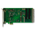
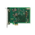
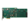
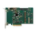
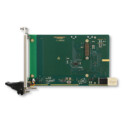
The TXMC639 is a standard single-width Switched Mezzanine Card (XMC) module that features a user-configurable FPGA (AMD Kintex™ 7) with up to 16 differential ADC input channels and up to 8 single-ended DAC output channels. The ADC input channels are based 16 bit 1.5 Msps LTC2320-16 ADC. Each channel has a 16 bit resolution and can operate at up to 1.5 Msps, with configurable differential input voltage ranges.
The DAC output channels are based on the Dual 16 bit AD5547 DAC. Each DAC output is configurable as a single-ended bipolar analog output with selectable voltage ranges.
The module also offers 32 ESD-protected TTL lines for a flexible digital interface, all individually programmable as input or output. Additionally, 16 of these TTL lines can be switched via the Board Configuration Controller (BCC) to provide 8 RS422 interfaces.
The module provides FPGA I/Os and Multi-Gigabit Transceivers for customer-specific I/O extension or inter-board communication.
The User FPGA is connected to a 1 GB DDR3L SDRAM, and the module comes with an FPGA Board Reference Design (BRD) loaded into the user FPGA by default. Configuration can be done through SPI flash, BCC, or JTAG interface, with support for PCIe specification compliance.
User applications for the TXMC639 with Kintex™ 7 FPGA can be developed using the AMD Vivado™ design tool. TEWS offers a well-documented FPGA Board Reference Design. It includes a constraint file with all necessary pin assignments and basic timing constraints. The FPGA Board Reference Design covers the main functionalities of the board.
The TXMC639 is delivered with the FPGA Board Reference Design. The FPGA could be programmed via the on-board Board Configuration Controller (BCC). Programming via JTAG interface using an USB programmer is also possible. In accordance with the PCI specification and the buffering of PCI header data, the contents of the user FPGA can be changed during operation.
TEWS Technologies is a partner at the highest level within the AMD Embedded Partner Program and offers FPGA Design and Integration services for all its FPGA solutions. The engineering team specializes in designing highly optimized FPGA designs and has extensive experience in minimizing FPGA gate usage. Having the FPGA custom designed according to the customer’s needs avoids overhead and delays leading to a reduction of costs for the customer.
PCI Express x4 Link (Base Specification 2.1) compliant interface conforming to ANSI/VITA 42.3-2006 (PCI Express Protocol Layer Standard)
PCI Express Switch
PI7C9X2G312GP (Pericom)
PCI Express to PCI Bridge
XIO2001 (Texas Instruments)
User configurable FPGA
TXMC639-10R: XC7K160T-2FBG676I (AMD)
TXMC639-11R: XC7K325T-2FBG676I (AMD)
SPI-Flash
MT25QL128 (Micron) 128 Mbit (contains TXMC639 FPGA BRD) or compatible; +3.3 V supply voltage
DDR3 RAM
2x MT41K256M16TW-107 (Micron) 256Meg x 32 bit
Board Configuration Controller
LCMXO2-7000HC (Lattice)
ADC
LTC2320 -16 (Analog Devices)
DAC
AD5547BRUZ (Analog Devices)
A/D Channels
TXMC639-10R: 8 Differential 16bit A/D Channels
TXMC639-11R: 16 Differential 16bit A/D Channels
Input Configuration per BCC Device:
Input Voltage Ranges:
Differental : ±20.57 V, ±10.28 V or ±5.14 V
(Single-Ended: ±10.28 V, ±5.14 V or ±2.57 V)
All analog inputs are connected via an impedance converter and a second operation amplifier for level adjustment and filtering to the differential ADC inputs.
The -3 dB limit of this input stage is at approx. 8MHz
D/A Channels
TXMC639-10R: 4 Single-Ended 16 Bit D/A Channels
TXMC639-11R: 8 Single-Ended 16 Bit D/A Channels
Output range configurable per D/A channel.
Simultaneous Conversion for all D/A Channels.
Maximum single-ended Output Voltage – Vout: ±10 V
Maximum Output Drive Current for each Output: 10 mA
Maximum Capacitive Load for each Output: 1000 pF
Typical Settling Time for a 10 mA / 1000 pF: < 1 µs
Digital Front I/O Channels
32 digital I/O Lines
Default configured as 32 ESD-protected TTL lines
16 I/O lines are configurable as 8 differential RS422 I/O lines with individual Termination enable.
Digital Rear I/O Channels
64 direct FPGA I/O lines to P14 Rear I/O connector
Can be used as single-ended or differential I/O
FPGA I/O Standard: LVCMOS25, LVTTL25 and LVDS25
4 MGT line to P16 Rear I/O connector
Each line consists of one differential RX and TX pair.
Transmission speeds of up to 3.125 Gb/s are possible.
Front I/O
Front I/O Samtec – ERF8_050_01_L_D_RA_L_TR
P14 Rear I/O
64 pin Mezzanine Connector (Molex 71436-2864 or compatible)
With TXMC639 Board Reference Design / without external load
typical @ +12 V VPWR
typical @ +5 V VPWR
TXMC639-10R
1.1 A
2.5 A
TXMC639-11R
1.3 A
3.3 A
Temperature Range
Operating: – 40 °C to + 85 °C
Storage: – 55 °C to + 125 °C
MTBF 1)
157 000 h to 161 000 h
Humidity
5% – 95% non-condensing
Weight
140 g
1) depends on variant, for further details see User Manual
PRODUCT VARIATIONS
TXMC639-10R
8x Analog In, 4x Analog Out, XC7K160T-2FBG676 Kintex™ 7 FPGA
AMD Kintex™ 7 FPGA (XC7K160T-2FBG676), 1GB DDR3, 8x Analog In, 4x Analog Out, 32x digital Front I/O, 64x direct FPGA Rear I/O Lines and 4x MGTs Rear I/O
TXMC639-11R
16x Analog In, 8x Analog Out, XC7K325T-2FBG676 Kintex™ 7 FPGA
AMD Kintex™ 7 FPGA (XC7K325T-2FBG676), 1GB DDR3, 16x Analog In, 8x Analog Out, 32x digital Front I/O, 64x direct FPGA Rear I/O Lines and 4x MGTs Rear I/O