TPMC541

32/16 Single-Ended or 16/8 Differential A/D Channels, 8/4 Voltage & Current Range D/A Channels and 8 LVTTL/TTL Digital I/O Channels

  • Standard single-width PMC module
  • up to 32 (single-ended) or 16 (differential) channel analog input
    • 16 bit A/D converter
    • Nearly simultaneous sampling
    • multiple analog input ranges (up to ±24.576 V)
    • Sequencer mode available
  • 8 channel analog output
    • Single-ended
    • 16 bit D/A converter
    • Simultaneous update
    • 0 V … 5 V, 0 V … +6 V, 0 V … +10 V and 0 V … +12 V unipolar voltage ranges
    • ±5 V, ±6 V, ±10 V and ±12 V bipolar voltage ranges
    • 0 mA … 20 mA, 4 mA … 20 mA, and 4 mA … 24 mA current ranges
    • Sequencer mode available
  • 8 channel digital I/O
    • Tri-state 5 V-tolerant LVTTL/TTL
    • Pull resistors to 3.3 V, 5 V, GND
  • DMA support
  • Factory calibration data available in EEPROM
  • Analog I/O hardware correction function available
  • external synchronization trigger signals via P14 I/O
  • Front panel I/O (Mini D Ribbon (MDR68) type connector)

Product status: Active

Operating Temperature Range -40 °C to +85 °C RoHS compliant

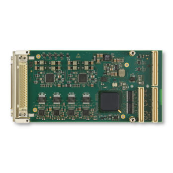
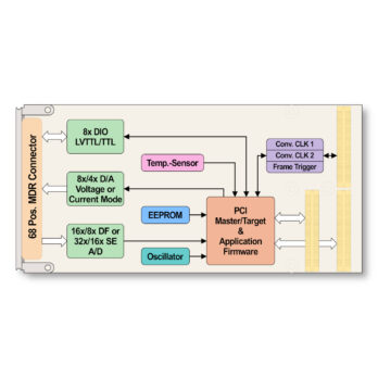
The TPMC541 is a standard single-wide PCI Mezzanine Card (PMC) compatible module providing:

  • A PCI Master capable 32 bit 33 MHz PCI interface
  • 8 Tristate-Capable bi-directional 5V-tolerant LVTTL/TTL compatible General Purpose Digital I/O Lines (Front I/O)
  • Up to 8 Single-Ended 16 bit Analog Outputs in (bipolar or unipolar) Voltage Mode or (unipolar) Current Mode (Front I/O)
  • Up to 32 Single-Ended or 16 Differential 16 bit bipolar Analog Inputs (Front I/O)
  • Tristate-Capable bi-directional 5V-tolerant LVTTL/TTL compatible Digital I/O Lines for Conversion Control Signals (Conversion Clock, Frame Trigger) (Rear-I/O)

Digital I/O

The TPMC541 features 8 ESD protected, interrupt and tristate-capable bi-directional general purpose digital I/O lines at the front I/O connector. Each digital I/O line features a pull resistor to a common reference (+3.3V, +5V or GND).

Analog Outputs

The TPMC541R-10R order option provides 8 (eight) analog output channels while the TPMC541R-20R order option provides 4 (four) analog output channels.

Each individual D/A channel can be configured to operate in any of the following output ranges:

  • 5V, 6V, 10V or 12V unipolar Voltage Ranges
  • ±5V, ±6V, ±10V or ±12V bipolar Voltage Ranges
  • 4mA to 20mA Current Range
  • 0mA to 20mA (or 24mA) Current Range

The TPMC541 provides a D/A Sequencer unit for performing periodic simultaneous digital to analog conversions at a configurable conversion rate.

Analog Inputs

The TPMC541R-10R order option provides 4 (four) ADAS3022 devices and up to 32 single-ended or 16 differential analog inputs. The TPMC541-20R order option provides 2 (two) ADAS3022 devices and up to 16 single-ended or 8 differential analog inputs.

Each ADC device configured for Single-Ended Input Configuration provides the following input voltage ranges (single-ended and referenced to ground): ±0.64V, ±1.28V, ±2.56V, ±5.12V, ±10.24V, ±12.288V.

Each ADC device configured for Differential Input Configuration provides the following differential input voltage ranges: ±0.64V, ±1.28V, ±2.56V, ±5.12V, ±10.24V, ±20.48V, ±24.576V.

The TPMC541 provides an A/D Sequencer unit for performing a sequence of periodic analog to digital conversions at a configurable conversion rate.

Conversion Correction Data

Each TPMC541 is factory calibrated. Conversion data correction values are determined during the factory acceptance test and are stored in an on-board serial EEPROM unique to each PMC module. These correction values may be used to perform a hardware correction for every individual D/A channel and output range and for every individual A/D channel and input range.

Conversion Control Signals

Conversion clock signals may be generated on-board for internal use and may also be driven out on P14 rear I/O if the card is operating as a master card in a Multi-Board configuration. The conversion clock signals may also be sourced externally via the P14 rear I/O interface if the card is operating as a slave card in a Multi-Board configuration.

I/O Connector

The general purpose digital I/O signals, the analog output signals and the analog input signals are accessible on a 68 pos. Mini D Ribbon (MDR68) front connector.
Mechanical Interface PCI Mezzanine Card (PMC) Interface confirming to IEEE P1386/P1386.1, Standard single-wide
Electrical Interface PCI Rev. 3.0 compatible, 33 MHz / 32 bit PCI Initiator/Target, 3.3V and 5V PCI Signaling Voltage compatible
FPGA Xilinx Spartan-6 FPGA
DAC TPMC541-10R: 2x AD5755-1 (Analog Devices)

TPMC541-20R: 1x AD5755-1 (Analog Devices)

ADC TPMC541-10R: 4x ADAS3022 (Analog Devices)

TPMC541-20R: 2x ADAS3022 (Analog Devices)

Digital I/O 74LVT126 (NXP)
FPGA Configuration Memory W25Q32 (Winbond) 32Mbit Serial SPI Flash
Correction Data EEPROM 16 kbit Serial EEPROM, M93C86-WMN6TP (ST)
D/A Channels TPMC541-10R: 8 Single-Ended 16 Bit D/A Channels

TPMC541-20R: 4 Single-Ended 16 Bit D/A Channels

D/A Channel

Output Range Options

Output range configurable per D/A channel.

Voltage Mode Ranges:
0V … 5V, 0V … 10V, -5V … +5V, -10V … +10V

Voltage Ranges available with 20% Overrange Mode:
0V … 6V, 0V … 12V, -6V … +6V, -12V … +12V
Up to 10mA load current per Voltage Mode D/A Channel

Current Mode Ranges:
4mA … 20mA, 0mA … 20mA, 0mA … 24mA
Max 680 Ω load resistance per Current Mode D/A Channel

D/A Conversion Rate Max. 38ksps Conversion Rate (all D/A Channels simultaneous)
A/D Channels TPMC541-10R: 4x ADAS3022 ADC Device

TPMC541-20R: 2x ADAS3022 ADC Device

A/D Channel Input Range Options Input Configuration per ADC Device:
8x Single-Ended A/D Channels or 4x Differential A/D ChannelsSingle-Ended Input Voltage Ranges:
±0.64V, ±1.28V, ±2.56V, ±5.12V, ±10.24V, ±12.228VDifferential Input Voltage Ranges:
±0.64V, ±1.28V, ±2.56V, ±5.12V, ±10.24V, ±20.48V, ±24.576V
A/D Conversion Rate On-board analog input 1st order low-pass filter with -3dB cutoff frequency of approx. 105kHz on all A/D channels

Max conversion Rate from 100ksps to 800ksps, depending on the number of active channels per ADC device.

(Pseudo-Simultaneous conversion for all A/D channels)

Digital I/O channels 8 ESD Protected TTL/LVTTL Digital I/O Lines (Front I/O) 3.3V Driver, 5V tolerant Receiver, Individual Output Enable Control, Pull Resistor to common reference, Programmable common pull resistor reference (3.3V, 5V, GND)

Up to 12mA Source Current and up to 6mA Sink Current per Digital I/O Line

Front I/O 68-pin Mini D Ribbon (MDR) (3M N10268-52E2PC or compatible)
P14 Back I/O 64-pin Mezzanine Connector (Molex 71436-2864 or compatible)
Power Requirements Only the 5V PMC Power Supply is used

TPMC541-10R: Typically 0.85A @ +5V DC without I/O Load
TPMC541-20R: Typically 0.55A @ +5V DC without I/O Load

I/O Load Calculation:

Add 0.005A @ +5V per active DIO Output Line
Add 0.070A @ +5V per active D/A Voltage Output w/o Overrange
Add 0.082A @ +5V per active D/A Voltage Output w/ Overrange
Add approx. (IRANGE_MAX2 * REXT) / 3V ampere @ +5V per active D/A Current Output

Temperature Range Operating: -40°C to +85°C (Forced air cooling is mandatory at ambient temperatures exceeding +40°C )
Storage: -40°C to +85°C
Weight 1) 82g to 86g
Humidity 5 – 95% non-condensing
MTBF 1) 165 000 h to 181 000h


1) depends on variant, for further details see User Manual

PRODUCT VARIATIONS

TPMC541-10R

32 Single-Ended or 16 Differential analog Inputs (16 bit), 8 Analog Voltage or Current Outputs (16 bit), 8 LVTTL/TTL I/O

32 single-ended or 16 differential analog inputs; 16 bit; simultaneous sampling; programmable ranges up to +/-24.576 V; 8 analog outputs (voltage / current); 16 bit; simultaneous update; programmable ranges up to +/-12 V or up to 24 mA; 8 LVTTL/TTL I/O; factory calibrated; Front I/O via MDR68 connector

TPMC541-20R

16 Single-Ended or 8 Differential analog Inputs (16 bit), 4 Analog Voltage or Current Outputs (16 bit), 8 LVTTL/TTL I/O

16 single-ended or 8 differential analog inputs; 16 bit; simultaneous sampling; programmable ranges up to +/-24.576 V; 4 analog outputs (voltage / current); 16 bit; simultaneous update; programmable ranges up to +/-12 V or up to 24 mA; 8 LVTTL/TTL I/O; factory calibrated; Front I/O via MDR68 connector

ACCESSORIES

MDR68 Cable

MDR68 Terminal Block

Cable Kit for Modules with MDR68 Connector

SOFTWARE

Device Driver for Multifunction Board Family (DAC, ADC and Digital I/O)

Data Sheet

Data Sheet

Data Sheet - Issue 1.0.0

User Manual

User Manual - Issue 1.0.1