TEWS Technologies Introduces High-Density Simulation PMC with 8 Analog Current Inputs, 16/8 Analog High-Voltage Inputs, 8 Analog Voltage/Current Outputs and 8 Digital LVTTL/TTL I/O
TEWS Technologies adds to its high-density embedded I/O product line with the introduction of the TPMC543, a standard 32-bit 33MHz single-wide PCI Mezzanine Card (PMC) module optimized for simulation applications and industrial control, traffic control and COTS requirements. The TPMC543 offers high density channels with current inputs, current outputs, high-voltage inputs, and standard voltage outputs in a single PMC module. Support of sensors for 2, 3, and 4-wire current transmitters and support of higher voltage analog inputs are featured.
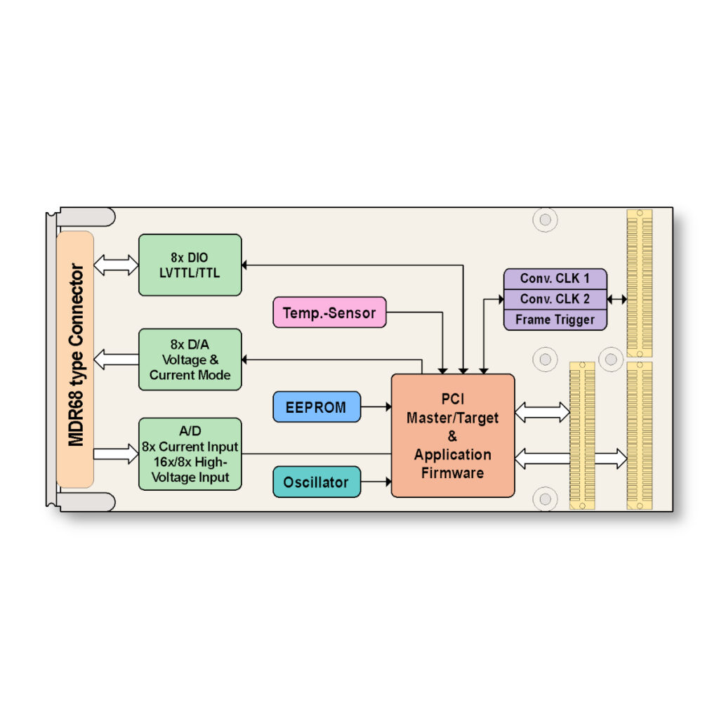
The TPMC543-10R features 4 multiplexed multi-channel 16 bit ADC devices, each device providing either 8 single-ended or 4 differential A/D channels.
On the TPMC543-10R the A/D channels are hardware- configured to provide:
- 8 differential bipolar analog current input channels with input range ±25mA
- 16 single-ended / 8 differential bipolar analog high-voltage input channels with single-ended up to ±48V and differential up to ±96V
The TPMC543-10R also features 2 multi-channel 16 bit DAC devices, providing a total of:
- 8 single-ended multi-mode analog output channels
Each individual D/A channel, is programmable for one of the following modes:
- Bipolar Voltage Output ±5V, ±6V, ±10V, ±12V
- Unipolar Voltage Output 0-5V, 0-6V, 0-10V, 0-12V
- Unipolar Current Output 4-20mA, 0-20mA, 0-24mA
Additionally, the TPMC543-10R provides 8 ESD protected tristate capable 5V-tolerant LVTTL/TTL digital input/output channels.
The TPMC543 provides dedicated A/D and D/A sequencer units for periodic analog-to-digital and digital-to-analog conversions at a configurable conversion rate. In sequencer mode, A/D conversion data is temporarily stored in an on-board data buffer and is transferred to system memory by PCI master DMA transfer while D/A conversion data is fetched from buffers in system memory by PCI master DMA transfer and is temporarily stored in an on-board data buffer. The sequencers provide a frame mode for repetitive frames of A/D and D/A conversions upon an internal or external trigger signal event.
Conversion clock (conversion rate) and frame trigger signals may be generated on-board for internal use and may also be driven out on P14 rear I/O if the card is operating as a master card in a multi-board configuration. The conversion clock (conversion rate) and frame trigger signals may also be sourced externally via the P14 rear I/O interface if the card is operating as a slave card in a multi-board configuration.
Each of the ESD protected digital I/O lines has a dedicated line transmitter with individual output enable control and a dedicated line receiver. The line receivers are always enabled, so the digital I/O line level can always be monitored. Each digital I/O line input can generate an interrupt triggered on rising edge, falling edge or both. Additionally, a glitch filter can be configured to get rid of bouncing on the digital I/O inputs. The individual digital I/O lines have a pull resistor to a common reference. The common pull resistor reference is programmable by software to +3.3V, +5V or GND.
Each TPMC543 is factory calibrated. The correction data is stored in an on-board serial EEPROM unique to each PMC module. The correction data values may be used for hardware correction for any A/D channel and input range and any D/A channel and output range.
The analog input, analog output and digital I/O signals are accessible via a Mini D Ribbon (MDR68) type front I/O connector.
Extensive software support for major operating systems such as Windows, Linux, VxWorks, Integrity and QNX is available.